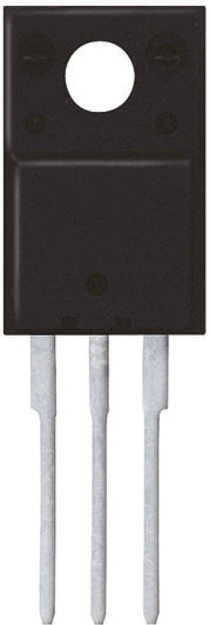
onsemi N-Channel MOSFET, 9 A, 500 V, 3-Pin TO-220F FQPF9N50CF

Technical Document
Specifications
Brand
onsemiChannel Type
N
Maximum Continuous Drain Current
9 A
Maximum Drain Source Voltage
500 V
Series
QFET
Package Type
TO-220F
Mounting Type
Through Hole
Pin Count
3
Maximum Drain Source Resistance
850 mΩ
Channel Mode
Enhancement
Minimum Gate Threshold Voltage
2V
Maximum Power Dissipation
44 W
Transistor Configuration
Single
Maximum Gate Source Voltage
-30 V, +30 V
Length
10.36mm
Typical Gate Charge @ Vgs
28 nC @ 10 V
Maximum Operating Temperature
+150 °C
Number of Elements per Chip
1
Width
4.9mm
Transistor Material
Si
Minimum Operating Temperature
-55 °C
Height
16.07mm
Product details
QFET® N-Channel MOSFET, 6A to 10.9A, Fairchild Semiconductor
Fairchild Semiconductor’s new QFET® planar MOSFETs use advanced, proprietary technology to offer best-in-class operating performance for a wide range of applications, including power supplies, PFC (Power Factor Correction), DC-DC Converters, Plasma Display Panels (PDP), lighting ballasts, and motion control.
They offer reduced on-state loss by lowering on-resistance (RDS(on)), and reduced switching loss by lowering gate charge (Qg) and output capacitance (Coss). By using advanced QFET® process technology, Fairchild can offer an improved figure of merit (FOM) over competing planar MOSFET devices.
MOSFET Transistors, ON Semi
ON Semi offers a substantial portfolio of MOSFET devices that includes high-voltage (>250V) and low-voltage (<250V) types. The advanced silicon technology provides smaller die sizes, which it is incorporated into multiple industry-standard and thermally-enhanced packages.
ON Semi MOSFETs provide superior design reliability from reduced voltage spikes and overshoot, to lower junction capacitance and reverse recovery charge, to elimination of additional external components to keep systems up and running longer.
Ideate. Create. Collaborate
JOIN FOR FREE
No hidden fees!


- Download and use our DesignSpark software for your PCB and 3D Mechanical designs
- View and contribute website content and forums
- Download 3D Models, Schematics and Footprints from more than a million products
₹ 712.05
₹ 142.41 Each (In a Pack of 5) (Exc. GST)
₹ 840.22
₹ 168.044 Each (In a Pack of 5) (inc. GST)
Standard
5
RS Components & Controls (I) Ltd
Distribution hub - B-89, Sector 67, Noida, Gautam Budh Nagar, (Uttar Pradesh), 201 301
₹ 712.05
₹ 142.41 Each (In a Pack of 5) (Exc. GST)
₹ 840.22
₹ 168.044 Each (In a Pack of 5) (inc. GST)
Standard
5
Stock information temporarily unavailable.
Please check again later.
| quantity | Unit price | Per Pack |
|---|---|---|
| 5 - 45 | ₹ 142.41 | ₹ 712.05 |
| 50 - 95 | ₹ 131.76 | ₹ 658.80 |
| 100 - 495 | ₹ 105.58 | ₹ 527.90 |
| 500 - 995 | ₹ 94.93 | ₹ 474.65 |
| 1000+ | ₹ 83.43 | ₹ 417.15 |
Ideate. Create. Collaborate
JOIN FOR FREE
No hidden fees!
- Download and use our DesignSpark software for your PCB and 3D Mechanical designs
- View and contribute website content and forums
- Download 3D Models, Schematics and Footprints from more than a million products
Technical Document
Specifications
Brand
onsemiChannel Type
N
Maximum Continuous Drain Current
9 A
Maximum Drain Source Voltage
500 V
Series
QFET
Package Type
TO-220F
Mounting Type
Through Hole
Pin Count
3
Maximum Drain Source Resistance
850 mΩ
Channel Mode
Enhancement
Minimum Gate Threshold Voltage
2V
Maximum Power Dissipation
44 W
Transistor Configuration
Single
Maximum Gate Source Voltage
-30 V, +30 V
Length
10.36mm
Typical Gate Charge @ Vgs
28 nC @ 10 V
Maximum Operating Temperature
+150 °C
Number of Elements per Chip
1
Width
4.9mm
Transistor Material
Si
Minimum Operating Temperature
-55 °C
Height
16.07mm
Product details
QFET® N-Channel MOSFET, 6A to 10.9A, Fairchild Semiconductor
Fairchild Semiconductor’s new QFET® planar MOSFETs use advanced, proprietary technology to offer best-in-class operating performance for a wide range of applications, including power supplies, PFC (Power Factor Correction), DC-DC Converters, Plasma Display Panels (PDP), lighting ballasts, and motion control.
They offer reduced on-state loss by lowering on-resistance (RDS(on)), and reduced switching loss by lowering gate charge (Qg) and output capacitance (Coss). By using advanced QFET® process technology, Fairchild can offer an improved figure of merit (FOM) over competing planar MOSFET devices.
MOSFET Transistors, ON Semi
ON Semi offers a substantial portfolio of MOSFET devices that includes high-voltage (>250V) and low-voltage (<250V) types. The advanced silicon technology provides smaller die sizes, which it is incorporated into multiple industry-standard and thermally-enhanced packages.
ON Semi MOSFETs provide superior design reliability from reduced voltage spikes and overshoot, to lower junction capacitance and reverse recovery charge, to elimination of additional external components to keep systems up and running longer.
Ideate. Create. Collaborate
JOIN FOR FREE
No hidden fees!
- Download and use our DesignSpark software for your PCB and 3D Mechanical designs
- View and contribute website content and forums
- Download 3D Models, Schematics and Footprints from more than a million products